 |
||||
|
||||

Technologies on Display
D3 - Nanotechnology and Nanostructured Materials for Electronics and Photonics
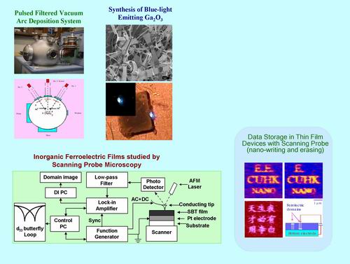
Electronic materials in the nanometer scale have very unique properties which are particularly important for future high performance electronic devices. In this project we aim to develop new nanosized materials and the relevant processing technologies for data storage and optical applications. We take advantage of the state-of-the-art ion-beam implantation and analysis facilities at CUHK to modify materials in order to generate new nanosized materials. In order to study the evolution of these materials under the influence of heat energy or during a chemical reaction, we use scanning probe techniques including atomic force microscopy (AFM) and scanning tunneling microscopy (STM) to image the atoms or nanosized features on the material surface.
Applications
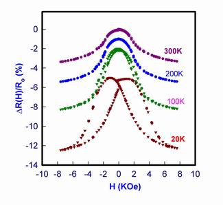
- Nanosized materials: High density magnetic and ferroelectric recording for nonvolatile memory, giant magneto-resistance, luminescent displays
- Nanometric processing and characterization technologies: synthesis of novel functional materials, surface modification, real-time imaging of atoms on surfaces
Features
- Ion-beam processing provides a non-equilibrium material synthesis route through which naturally uncommon but highly functional material phases can be created
- Some of these materials have extremely high magnetic / ferroelectric / luminescence figures of merit
- Scanning probe technique offers ultra-high resolution on sub-atomic scale
Principal Investigators
Prof. S. P. Wong / Prof. J. B. Xu
Department of Electronic Engineering