 |
||||
|
||||
Technologies on Display
D1 - Photonic Packaging
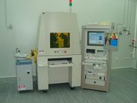
The Photonic Packaging Laboratory (PPL) was established in 2001 through the support of Innovation and Technology Fund and local industries. It aims to develop advanced packaging technologies and processes for photonic components. The main site is a class 1,000 clean room located in LG1, Science Center North, CUHK. It has the most state-of-the art research equipment including optical coating system, laser welding system, automatic alignment system, wafer scriber, die bonder, wire bonder etc. The missions of PPL are to support R & D in photonic industry and academics, to provide technical training, and technology transfer on packaging process for photonic devices
Applications
Examples of technologies that we have developed and devices that we have
packaged include:
- Antireflection (AR) /High reflection (HR) dielectric coatings
- Optical detectors and laser diodes with fiber pigtailing
- Semiconductor optical amplifier module
Ongoing projects
- MEMS optical switches module
- Multi-component packaging development
Services
- R&D facilities available to local industry through contract services or joint projects
- Prototype development
- Manpower training on photonic packaging processes
Website
http://www.erg.cuhk.edu.hk/PPL
Principal Investigators
Prof. Hon Tsang / Chester Shu
Department of Electronic Engineering
Projector Co-ordinator
Prof. Frank Tong
Department of Information Engineering
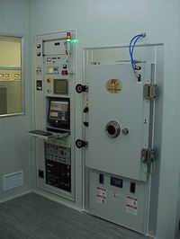
Optical Coating System
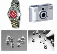
Multi-layer thin film coatings have several functions: AR, UV and IR cut, or
other optical effects.
Applications can be found in watches, camera lens, ball lens, display and
etc.
Laser Welding System
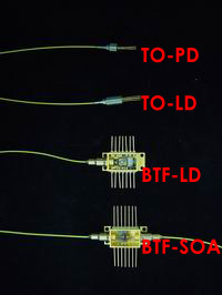
Active alignment technique using Laser Welding System can be applied to
package different types of photonic devices. TO-can and butterfly (BTF)
packages are common configurations for laser diode (LD), photodiode (PD) and
semiconductor optical amplifier (SOA).